New Features Improve Collaboration in SOLIDWORKS PCB 2019
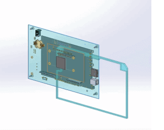 When you design a PCB (Printed Circuit Board) there are often times when you need to create barriers or height restrictions for component placements as envelopes. To do that, you can place a component called envelope. Once placed, you can change the component properties to be an envelope. You can then mate it into the position where you want the envelope to be placed on your printed circuit board.
Once complete, you can then push the changes to SOLIDWORKS PCB using Collaboration and pull the change with the addition of the envelope. You can preview the changes, accept them, and the envelope will be placed on the board in the exact location as in mCAD. Later, you can add chamfers in the upper corners to match the additions. This is a powerful and efficient way to create restrictions inside of SOLIDWORKS mechanical and push them over for collaboration with SOLIDWORKS PCB 2019.
Import thickness into a design
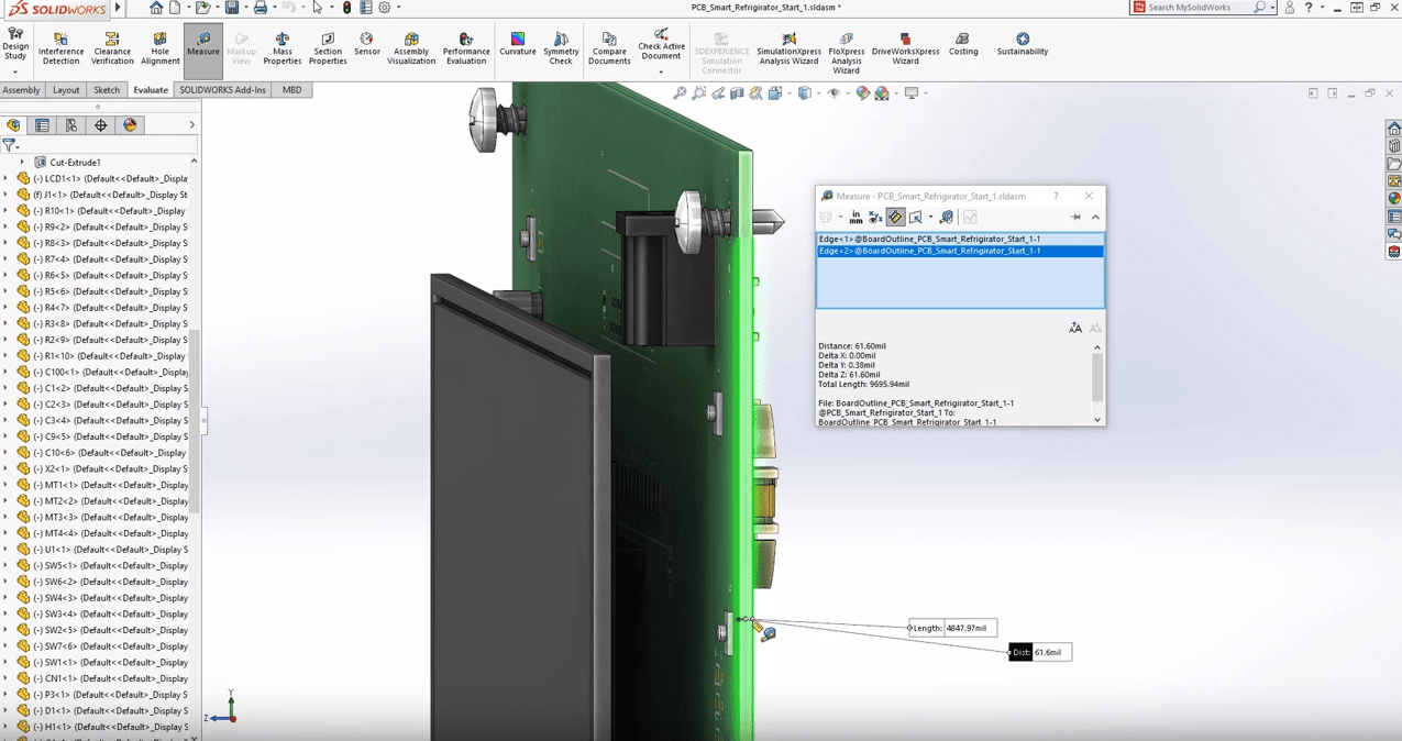
If the board thickness and representation between eCAD and mCAD is not accurately modeled, then you can’t trust your 3D board assembly. In SOLIDWORKS PCB 2019, we have the ability to import thickness into a design. Simply go into Layer Stack Manager and see that the board is defined as 16.2 mil thick. Using PCB collaboration we can transfer the design to SOLIDWORKS Mechanical where it accurately transforms the board thickness. If we go into Measure, we can see that it is exactly at the 16.2 mil that we defined in PCB.
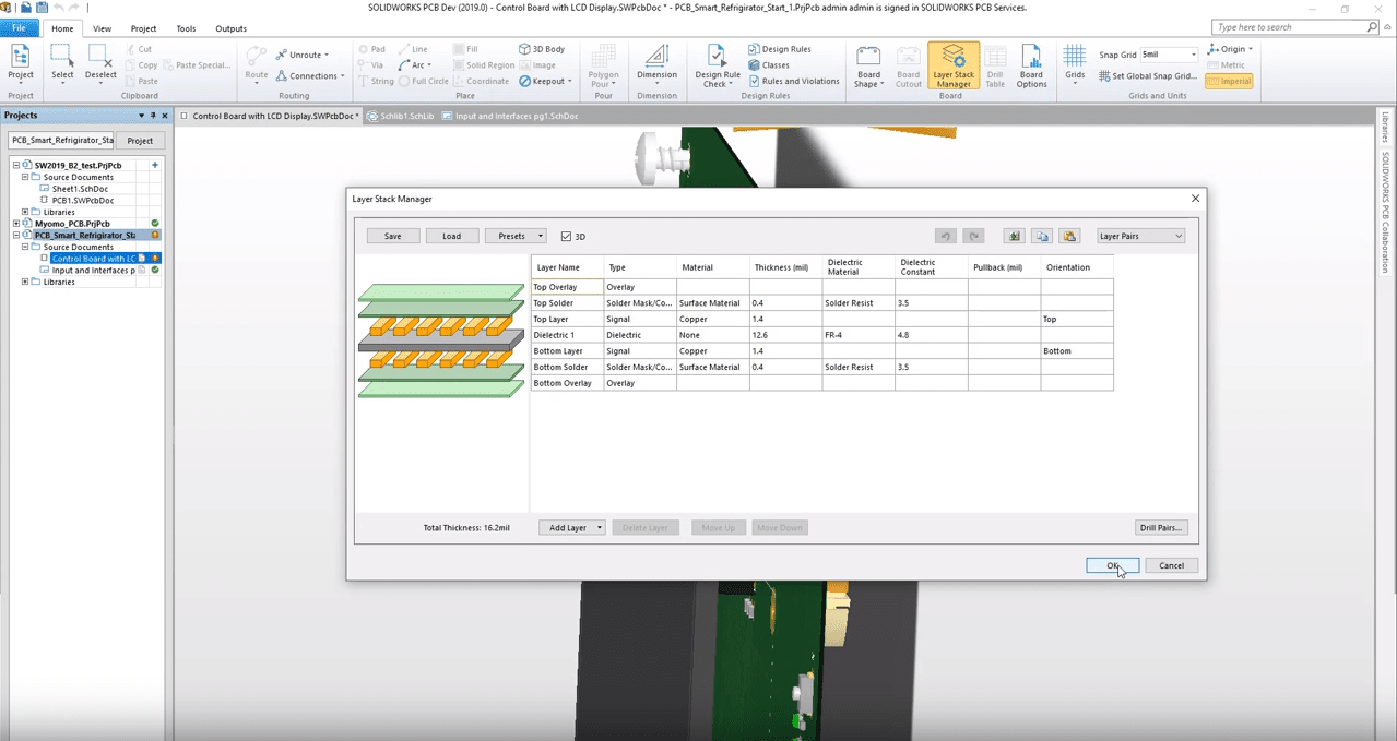
Going back to SOLIDWORKS PCB, we can increase the thickness of the board by changing the dielectric thickness to 58 mils which will bring the overall thickness of the board to 61.6 mils. Using PCB collaboration, you can push design changes of the board thickness. Back in SOLIDWORKS Mechanical, we are going to pull changes and preview them. You can accept the changes and the board thickness is increased. You can, again, verify the board thickness with the measure tool and verify that it is the 16.6 mils that you changed it to. This accurate board thickness representation in eCAD and mCAD eliminates possible errors and accurately models the board assembly.
Searching for projects is now easier
SOLIDWORKS Mechanical can connect to SOLIDWORKS PCB using the collaboration services. Selecting it and initializing the first pull will open the project list. The list can often be long and finding the right project takes some time. In SOLIDWORKS 2019 you can sort projects by the last modified column or you can go into captions and search for a different project.
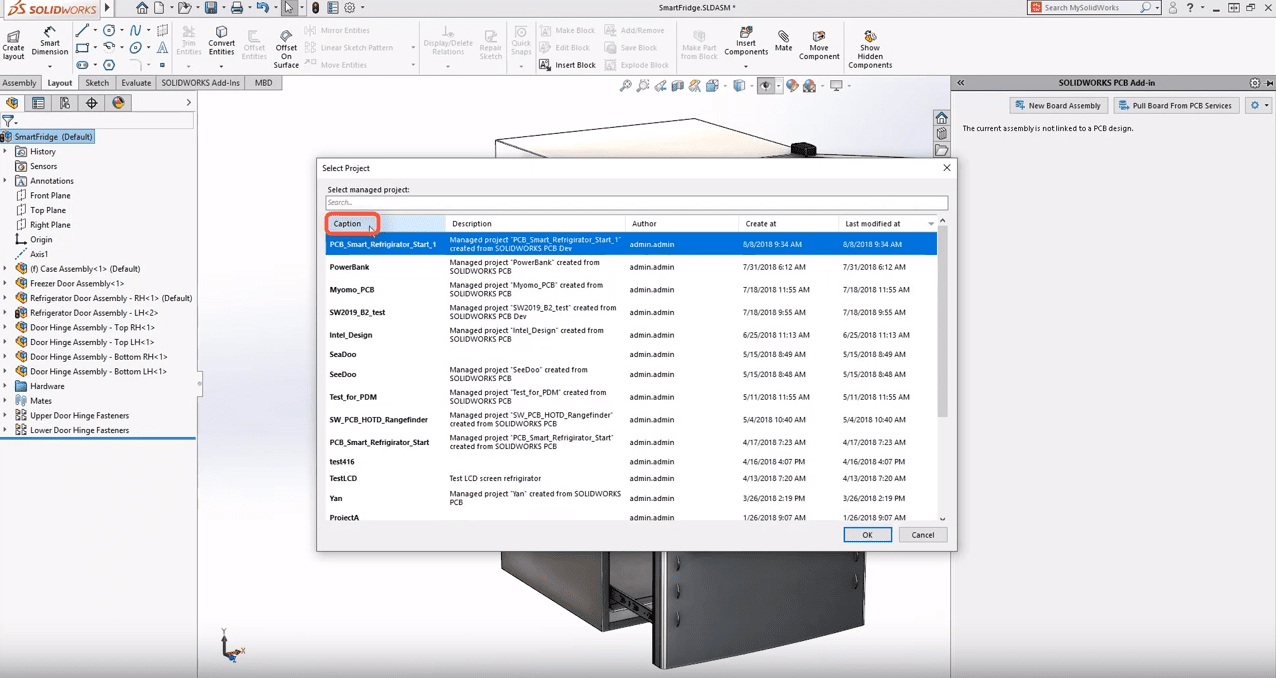
You can additionally search by either a partial or actual name. If you start typing it will update the search to show only the content you have entered enabling you to find projects quickly and start collaborating.
To see these new features in SOLIDWORKS PCB 2019 in action, watch the video below.
Related Articles
Get a Sneak Peak of SOLIDWORKS 2019
SOLIDWORKS MBD 2019: New Security Settings and More
What’s New in eDrawings 2019 | SOLIDWORKS 2019
About the Author
 Angelle Erickson writes about how companies are using innovative technologies, such as 3D printers and SOLIDWORKS software to increase productivity, improve product development processes, and maximize business potential.

 Blog
Blog 